We are surrounded by devices, that we use in our day to day life such as TVs, Cameras, Cell Phones, Telephones, WiFi, Internet, Antennas, etc. The power of Circuits, and Integrated Circuits have enabled humanity to function easier with the Semiconductor technological revolution.
Integrated Circuits "ICs", commonly referred as "Chips" have revolutionized the semiconductor industry since the invention of Complimentary MOS (CMOS), as well as ICs.
 |
| Fig: First IC design invention - A patent from 1960s by Jack Kilby (Photo Credits: A picture/poster I pasted on the wall by my computer desk). |
There are two types of ICs: Analog, and Digital ICs. Although their is a high increasing demand of Digital Integrated Circuits, the Analog ICs have been increasing in demand considerably, if not as equal as Digital ICs. Yes, you won't stay unemployed if you are into analog circuits, although majority of devices around us are "digital" hinting us to get employed and design digital circuits.
This article is majorly focused on CMOS Analog ICs. Only proceed further reading this article if Analog Circuit Design sparks your interest.
CMOS Technology Highlights:
- Dominant technology in the industry to fabricate ICs.
- Reliable, manufacturable, scalable, low power consumption, low cost.
- Used in VLSI or ULSI circuit chips.
- CMOS IC Design Process:
- Consists of defining circuit inputs and outputs, hand calculations, circuit simulations, circuit layout, simulations including parasitics, reevaluation of circuit input & output, fabrication, and testing.
- The CMOS IC design process is dependent on the current market, and customer needs. The design specifications alter as the need changes. This design alteration is performed by the result of trade-offs made between cost and performance.

Fabrication:
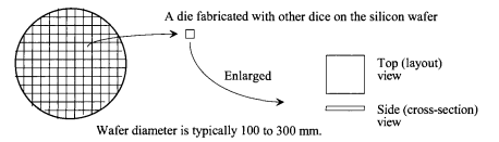
FIG(image source - CMOS circuit design, layout, and simulation by R. Jacob Baker IEEE Press): CMOS integrated circuits are fabricated on and in a silicon wafer.
- The process of CMOS IC fabrication is processed over thin circular slices of silicon called wafers of diameter 300mm/12inch containing several identical chips or die.
- MOSIS: http://mosis.com
- A pioneer service in manufacturing and fabricating MPW (Multi Project Wafer). The fabrication after design and layout can be performed through MOSIS.
- The chip's electrical signals are transmitted to the pins of package through wires, called "bond wires" electrically bond the chip to package and pins of the chip are electrically connected/shorted to a piece of metal on the chip called a bonding pad. The chip is held in the cavity of the package with an epoxy resin/glue.
- To mass produce these chips, instead of using ceramic packages, plastic packages are used (except where chips dissipate a lot of heat or the chips that are placed directly on the PCB). Plastic encapsulated chips are placed on a lead frame and then encapsulate the die and lead frame in plastic which is melted around the chip. The chip's leads are bent to the correct position after packaging, followed by printing the chip type, manufacturer, lot number information on the chip.
- CMOS circuit design (origin - Fairchild Semiconductor): The novel idea of using PMOS and NMOS will be discussed in the upcoming post — STAY TUNED!!
Comments
Post a Comment