PCIe - TLP Header, Packet Formats, Address Translation, Config Space, Command Register, Configuration types
TLP Packet Format:
TLP Header:
Status Register:
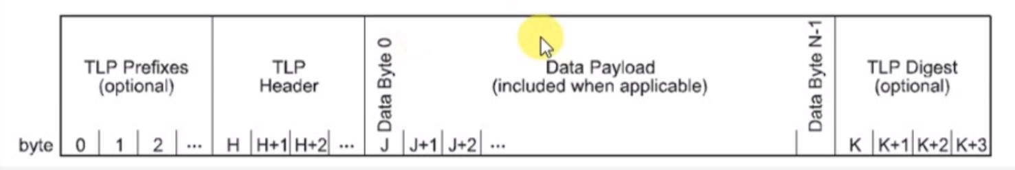 |
| FIG: TLP Packet Format. |
- The Transaction Layer Packet Format is defined as:
- Starts with a Prefix, which is an optional one and,
- TLP Header and then,
- With/Without Data Payload,
- At the end of TLP Packet a TLP Digest,
- The information in TLP Packet Format is distributed as:
- TLP Prefixes.
- Header (mandatory).
- Data (included when applicable): depends on the transaction type.
- TLP Digest (optional).
 |
| FIG: TLP Byte Information |
- Provides Format of the packet.
- Type of the packet.
- Length of associated data, if available.
- Transaction Descriptor.
- Address/Routing information
- Byte enables
- Message encoding
- Completion Status
 |
| FIG: Common TLP Header. |
- 32-bit if information.
- Provides: Format, TLP Packet Type, Traffic Class info, Attributes, T Heads (Presence of TLP Prefix, if present), TLP Digest, End Point (TLP is Normal or Poisoned), Address Translation (When memory is available). Length (Data Length notation denoted in 32bit words)
- Fmt and Type define the Length of a Packet.
Packet format & Type Encoding:
Some additional Transaction types are as follows:-
TLP Type
|
Format
|
||
TLP Length Encoding:
- DW: D Words.
- All 1s: 1023 D Words.
- All 0s: 1024 D Words are present in the packet.
- Suppose there are 1024 D Words of data, then the Root Complex will divide the data into smaller packets and send them to the EndPoints. If there is a Switch present in between, then the data is forwarded as it is without splitting it into the packets or without any change.
Address Formats:
 |
| FIG: 64-bit Address Routing |
 |
| FIG: 32-bit Address Routing |
Address Translation:
Default / Untranslated
|
|
01
|
Translation Request
|
10
|
Translated
|
11
|
Reserved
|
Routing:
 |
| FIG: ID Routing with 4 DW Header |
 |
| FIG: ID Routing with 3 DW Header |
- Data uses Routing information like, Bus Number; Device Number, Function Number, etc to reach a particular endpoint.
- The Routing type (3 or 4 D Words of Header) depends on the need of TLP digest.
- The Switch checks for Bus Number and Device Number and it forwards the packet to that particular endpoint accordingly in order to perform the Routing during the Run-Time.
PCIe Configuration Space:
 |
| FIG: Configuration Space. |
- 4KB of Space.
- Starts from 0 to fff.
- 0 to 255 (256B) of PCIe Config Space.
- from 100 to fff of Extended PCIe Configuration Space.
- While defining legacy PCI compatible mode and O.S., this kind of (0-fff) space is not available.
- 0-3f is PCIe Compatibility Configuration Space.
- PCIe Capability Structure determines if Entended Configuration space for PCI is present or not.
- 0-ff PCI Configuration Space is analogous to PCIe-PCI and it has different kinds of information.
- Configuration Space can be either of Type-0 or Type-1.
 |
| FIG: Type 0 / 1 Configuration Space |
- Type 0: Used for Endpoints.
- Type 1: Used for Switches and Root Complex.
- Common information provided for both type 0/1 is shown above.
- Identification Registers:
- Device ID:
- Device unique identification value.
- Vendor ID:
- Vendor unique identification value.
PCIe ConfigSpace Command Register:
Status Register:
Interrupt Status
|
Set indicates INTx emulation interrupt is pending or if it has been processed by the CPU or Root Complex
|
|
Capabilities List
|
Indicates presence of Extended PCIe capability list
|
|
66MHz
|
N/A to PCIe
|
|
Fast back-to-back enable
|
N/A to PCIe
|
|
Master Data Parity Error
|
Set by endpoint if parity error response bit in Command Register received by the endpoint
|
|
DEVSEL (Device Select) timing
|
N/A to PCIe
|
|
Signaled Target Abort
|
Set when a function completes as a Completor Abort Error
|
|
Received Target Abort
|
Set when function receives completion with abort
|
|
Received Master Abort
|
Set when requester receives a completion with unsupported request completion status
|
|
Signaled System Error
|
Set when the function sends a fatal or non-fatal error message
|
|
Detected Parity Error
|
Set when function receives poisoned TLPs
|
Registers:
- Cache Line Register
- Latency Timer Register
- Interrupt Line Register
- Interrupt Pin Register
- Error Register
PCI Type-0 Configuration Space:
 |
| FIG: Type 0 PCI Configuration Space |
- BAR (Base Address Registers) space is used to map the internal functions or internal memory requests into the corresponding system memory.
- To summarize, Base Address Registers or BAR (offset 10h - 24h)
- Resources are mapped into memory space using BAR registers.
- Supports 64bit addressing for any BAR request prefetchable memory.
- Minimum memory space range requested is 128 Bytes. Whenever we are Writing into that BAR Register and Read Back the information, whatever size it supports will be set to 1 and others to 0. With this, we can come to a conclusion of BAR base address 0 and if it needs to be allocated or not (BAR = 0 implies Not in Use).
- Minimum Grant / Maximum Latency Registers (offset 3Eh / 3Fh)
- N/A to PCIe, Hardwired to 00h.
PCI Type-1 Configuration Space:
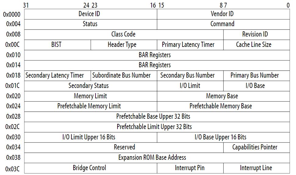 |
| FIG: Type 1 PCI Configuration Space |
- Registers:
- Base Address Register (offset 10h / 14h)
- Primary Bus Number (Root Complex - 0)
- Secondary Bus Number (Enumerated during the runtime)
- Secondary Latency Timer (N/A for PCIe)
- Secondary Status Register (similar to Common Status Register)
- Prefetchable Memory Base / Limit
- Bridge Control Register (used for bridging PCIe to PCI)
*To know more about PCI and PCI Express in detail, you can refer the documentation of Intel's user guide.
Helpful facts
ReplyDeleteAmazing! You have Shared great content here... I am glad to discover this post as I found lots of valuable data in your article. Thanks a lot keep posting :)
ReplyDeleteBitcoin Mining Machines
why TLP header format is starts from Byte 0 to byte N any particular reason
ReplyDeleteNice
ReplyDeletehow/where do we use TLP prefix?
ReplyDeleteThank you for being you
ReplyDeleteNice post thanks ffor sharing
ReplyDelete