PCIe - TLP Header, Packet Formats, Address Translation, Config Space, Command Register, Configuration types
TLP Packet Format:
TLP Header:
Status Register:
 |
| FIG: TLP Packet Format. |
- The Transaction Layer Packet Format is defined as:
- Starts with a Prefix, which is an optional one and,
- TLP Header and then,
- With/Without Data Payload,
- At the end of TLP Packet a TLP Digest,
- The information in TLP Packet Format is distributed as:
- TLP Prefixes.
- Header (mandatory).
- Data (included when applicable): depends on the transaction type.
- TLP Digest (optional).
 |
| FIG: TLP Byte Information |
- Provides Format of the packet.
- Type of the packet.
- Length of associated data, if available.
- Transaction Descriptor.
- Address/Routing information
- Byte enables
- Message encoding
- Completion Status
 |
| FIG: Common TLP Header. |
- 32-bit if information.
- Provides: Format, TLP Packet Type, Traffic Class info, Attributes, T Heads (Presence of TLP Prefix, if present), TLP Digest, End Point (TLP is Normal or Poisoned), Address Translation (When memory is available). Length (Data Length notation denoted in 32bit words)
- Fmt and Type define the Length of a Packet.
Packet format & Type Encoding:
Some additional Transaction types are as follows:-
TLP Type
|
Format
|
||
TLP Length Encoding:
- DW: D Words.
- All 1s: 1023 D Words.
- All 0s: 1024 D Words are present in the packet.
- Suppose there are 1024 D Words of data, then the Root Complex will divide the data into smaller packets and send them to the EndPoints. If there is a Switch present in between, then the data is forwarded as it is without splitting it into the packets or without any change.
Address Formats:
 |
| FIG: 64-bit Address Routing |
 |
| FIG: 32-bit Address Routing |
Address Translation:
Default / Untranslated
|
|
01
|
Translation Request
|
10
|
Translated
|
11
|
Reserved
|
Routing:
 |
| FIG: ID Routing with 4 DW Header |
 |
| FIG: ID Routing with 3 DW Header |
- Data uses Routing information like, Bus Number; Device Number, Function Number, etc to reach a particular endpoint.
- The Routing type (3 or 4 D Words of Header) depends on the need of TLP digest.
- The Switch checks for Bus Number and Device Number and it forwards the packet to that particular endpoint accordingly in order to perform the Routing during the Run-Time.
PCIe Configuration Space:
 |
| FIG: Configuration Space. |
- 4KB of Space.
- Starts from 0 to fff.
- 0 to 255 (256B) of PCIe Config Space.
- from 100 to fff of Extended PCIe Configuration Space.
- While defining legacy PCI compatible mode and O.S., this kind of (0-fff) space is not available.
- 0-3f is PCIe Compatibility Configuration Space.
- PCIe Capability Structure determines if Entended Configuration space for PCI is present or not.
- 0-ff PCI Configuration Space is analogous to PCIe-PCI and it has different kinds of information.
- Configuration Space can be either of Type-0 or Type-1.
 |
| FIG: Type 0 / 1 Configuration Space |
- Type 0: Used for Endpoints.
- Type 1: Used for Switches and Root Complex.
- Common information provided for both type 0/1 is shown above.
- Identification Registers:
- Device ID:
- Device unique identification value.
- Vendor ID:
- Vendor unique identification value.
PCIe ConfigSpace Command Register:
Status Register:
Interrupt Status
|
Set indicates INTx emulation interrupt is pending or if it has been processed by the CPU or Root Complex
|
|
Capabilities List
|
Indicates presence of Extended PCIe capability list
|
|
66MHz
|
N/A to PCIe
|
|
Fast back-to-back enable
|
N/A to PCIe
|
|
Master Data Parity Error
|
Set by endpoint if parity error response bit in Command Register received by the endpoint
|
|
DEVSEL (Device Select) timing
|
N/A to PCIe
|
|
Signaled Target Abort
|
Set when a function completes as a Completor Abort Error
|
|
Received Target Abort
|
Set when function receives completion with abort
|
|
Received Master Abort
|
Set when requester receives a completion with unsupported request completion status
|
|
Signaled System Error
|
Set when the function sends a fatal or non-fatal error message
|
|
Detected Parity Error
|
Set when function receives poisoned TLPs
|
Registers:
- Cache Line Register
- Latency Timer Register
- Interrupt Line Register
- Interrupt Pin Register
- Error Register
PCI Type-0 Configuration Space:
 |
| FIG: Type 0 PCI Configuration Space |
- BAR (Base Address Registers) space is used to map the internal functions or internal memory requests into the corresponding system memory.
- To summarize, Base Address Registers or BAR (offset 10h - 24h)
- Resources are mapped into memory space using BAR registers.
- Supports 64bit addressing for any BAR request prefetchable memory.
- Minimum memory space range requested is 128 Bytes. Whenever we are Writing into that BAR Register and Read Back the information, whatever size it supports will be set to 1 and others to 0. With this, we can come to a conclusion of BAR base address 0 and if it needs to be allocated or not (BAR = 0 implies Not in Use).
- Minimum Grant / Maximum Latency Registers (offset 3Eh / 3Fh)
- N/A to PCIe, Hardwired to 00h.
PCI Type-1 Configuration Space:
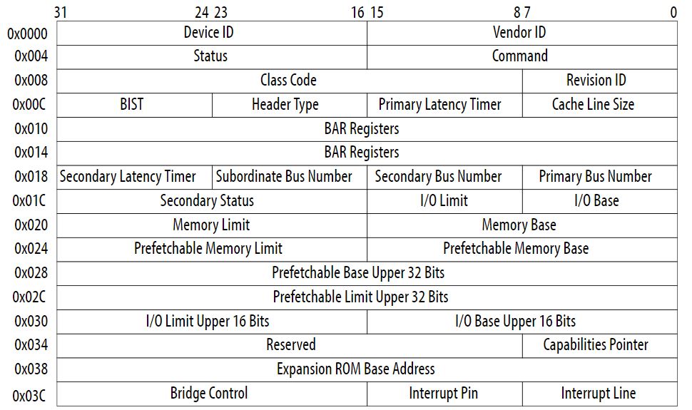 |
| FIG: Type 1 PCI Configuration Space |
- Registers:
- Base Address Register (offset 10h / 14h)
- Primary Bus Number (Root Complex - 0)
- Secondary Bus Number (Enumerated during the runtime)
- Secondary Latency Timer (N/A for PCIe)
- Secondary Status Register (similar to Common Status Register)
- Prefetchable Memory Base / Limit
- Bridge Control Register (used for bridging PCIe to PCI)
*To know more about PCI and PCI Express in detail, you can refer the documentation of Intel's user guide.
Helpful facts
ReplyDeleteAmazing! You have Shared great content here... I am glad to discover this post as I found lots of valuable data in your article. Thanks a lot keep posting :)
ReplyDeleteBitcoin Mining Machines
This is a well-structured technical article that simplifies the complex concepts of PCI Express communication by explaining TLP headers, packet formats, address translation, and configuration space. The detailed descriptions and protocol breakdown make it an excellent learning resource for students and professionals interested in modern hardware interfaces and high-speed digital communication.
DeleteA strong understanding of PCIe architecture and hardware communication protocols is essential for designing reliable electronic and embedded systems. Students working on IEEE Projects of ECE can apply these concepts while developing high-performance hardware interfaces, digital systems, and communication-based applications.
Learning different Domains in ECE Engineering helps students explore advanced topics such as digital electronics, processor interfaces, communication protocols, and system design, enabling them to build innovative solutions for modern electronic and embedded applications.
Deletewhy TLP header format is starts from Byte 0 to byte N any particular reason
ReplyDeleteNice
ReplyDeletehow/where do we use TLP prefix?
ReplyDeleteThank you for being you
ReplyDeleteNice post thanks ffor sharing
ReplyDelete